Now Reading: Indian scientists submit detailed project report to develop new semiconductor material | India News
-
01
Indian scientists submit detailed project report to develop new semiconductor material | India News

Indian scientists submit detailed project report to develop new semiconductor material | India News

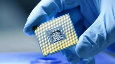
NEW DELHI: A staff of 30 scientists from India’s premier institute, the Indian Institute of Science (IISc), has submitted a proposal to the federal government to develop ‘angstrom-scale’ chips, far smaller than the smallest chips at the moment in manufacturing. The staff has submitted the proposal to the federal government for creating applied sciences utilizing a new class of semiconductor supplies, known as 2D Materials, that might allow chip sizes as small as one-tenth of the smallest chips at the moment in international manufacturing and develop India’s management in semiconductors.
Currently, semiconductor manufacturing is dominated by silicon-based applied sciences, led by superior nations such because the US, Japan, South Korea, and Taiwan.
“A team of scientists at IISc submitted a detailed project report (DPR) to the Principal Scientific Adviser (PSA) in April 2022, which was revised and submitted again in October 2024. The report was later shared with the Ministry of Electronics and IT. The project promises to develop angstrom-scale chips, far smaller than the smallest chips in production today,” a supply within the authorities aware of the proposal instructed PTI.
The DPR proposes the event of 2D semiconductors utilizing ultra-thin supplies like graphene and transition metallic dichalcogenides (TMDs). These supplies can allow chip fabrication on the angstrom scale, considerably smaller than present nanometer-scale applied sciences.
The smallest chip at the moment in manufacturing is the 3-nanometer node, manufactured by firms like Samsung and MediaTek.
A quick abstract of the 2D supplies project — which goals to substitute silicon, is accessible on the web site of the PSA’s workplace.
Sources within the Ministry of Electronics and IT (MeitY) confirmed that the proposal has been underneath dialogue.
“MeitY is positive about the project. The Principal Scientific Adviser and Secretary, MeitY, have held meetings on it. MeitY is exploring the electronics applications where such technology can be deployed. This is a collaborative effort that requires due diligence at every step,” an official conscious of the matter mentioned.
India at the moment depends closely on international gamers for semiconductor manufacturing — a know-how that’s strategic from each an financial and nationwide safety standpoint.
The nation’s largest semiconductor project, being arrange by Tata Electronics in partnership with Taiwan’s PSMC, entails an funding of Rs 91,000 crore. This project has been accepted underneath the India Semiconductor Mission and is eligible for 50 per cent capital assist from the federal government.
In comparability, the IISc-led proposal requests a comparatively modest Rs 500 crore over 5 years to construct indigenous know-how for next- technology semiconductors. The project additionally features a roadmap for self-sustainability after the preliminary funding section.
Globally, 2D supplies have drawn important curiosity. Europe has invested over USD 1 billion (round Rs 8,300 crore), South Korea over USD 300 million, and international locations like China and Japan have made severe however undisclosed investments in 2D material-based semiconductor analysis.
“2D materials will be key enablers for future heterogeneous systems. While global momentum is building, India’s efforts remain limited and need urgent scaling. This is a domain where India can take leadership, but time is running out,” mentioned an officer aware of the efforts and international developments, talking on situation of anonymity.
According to the PSA workplace web site, communications concerning the project have been ongoing since 2021, with outreach to key ministries together with MeitY, DRDO, and the Department of Space. NITI Aayog additionally really helpful the project in September 2022 primarily based on the IISc report.
The officer privy to the analysis ecosystem famous that a number of international locations are already getting ready for a post-silicon world as conventional chip scaling nears its limits.
“Global technology players have turned their attention to 2D semiconductors. India now needs to move from deliberation to execution. The proposal seeks Rs 500 crore over five years, but there is still no formal assurance. This window may not stay open for long,” the particular person added.


